

Fed Rate Hike September 2026: What It Means for India
The US Fed raised rates by 25 bps to 3.75%-4.00% in September 2026. See why it hiked, what...
17 September 2026

Finnovate’s editorial team researches and creates financial content using trusted sources, regulatory references and inputs from subject experts.
India's semiconductor story has usually been told through one question: When will the country get its first large-scale chip fab?
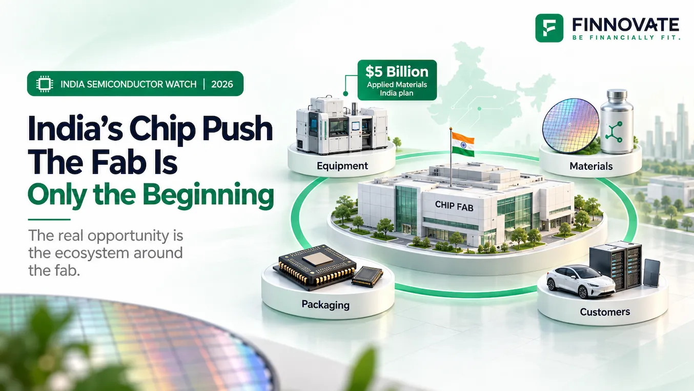
That question still matters. Tata Electronics is building a $11 billion, 300 mm semiconductor fab at Dholera in Gujarat, with planned capacity of about 50,000 wafers per month. But one of the more important announcements from SEMICON India 2026 did not involve another fab.
Applied Materials announced plans to invest $5 billion in India through 2035, focused on research, workforce development and building a deeper semiconductor supply chain. The company also plans to expand its India-based supply-chain capacity tenfold. Separately, Nexperia and Tata Electronics announced plans covering chip fabrication at Dholera and assembly and testing at Tata's Jagiroad facility in Assam.
These developments point towards a broader shift.
That distinction may determine whether India ends up with a few subsidised semiconductor plants or develops an industry that can sustain itself.
Table of Contents
The term "semiconductor manufacturing" often gets reduced to wafer fabrication.
In reality, a finished chip passes through a much larger chain.
| Stage | What happens |
|---|---|
| Chip design | Engineers decide what the chip should do and design its circuits |
| Equipment & materials | Highly specialised machines, chemicals, gases and wafers are prepared |
| Wafer fabrication | Microscopic circuits are built layer by layer on silicon wafers |
| Packaging & testing | Chips are cut, connected, protected and tested |
| End use | Finished chips go into cars, phones, data centres, factories and other products |
A wafer fab may be the most expensive individual facility in this chain.
But the fab cannot operate competitively without the layers surrounding it.
It needs lithography machines, deposition and etching equipment, ultra-pure chemicals, specialty gases, spare parts, process engineers, packaging companies and customers willing to place commercial orders.
This is why the Applied Materials announcement matters.
Applied Materials is one of the major global suppliers of semiconductor-manufacturing equipment.
Its machines are used during several stages of wafer processing, including adding, modifying and removing extremely thin layers of material as chips are fabricated.
The company's new India plan involves $5 billion of investment over roughly a decade, with emphasis on engineering, research, supplier development and workforce expansion rather than constructing its own chip fab. It has also said it intends to increase India-based supply-chain capacity tenfold by 2035.
That may look less dramatic than announcing another multibillion-dollar wafer plant.
But semiconductor fabs need companies such as Applied around them.
India can subsidise construction of a fab. It cannot simply subsidise its way into having hundreds of qualified precision suppliers overnight.
That supplier network has to develop through engineering capability, quality control, customer qualification and repeated manufacturing experience.
The new commitment is an expansion of an existing strategy.
Applied Materials already has engineering and R&D operations in India and had previously announced a collaborative engineering centre in Bengaluru focused on semiconductor-manufacturing equipment and supplier development.
The 2026 plan substantially increases that commitment.
More importantly, Applied is no longer the only major semiconductor-equipment company becoming involved in India's manufacturing build-out.
At SEMICON India 2026, Lam Research announced approximately ₹10,000 crore for its first Indian silicon-component manufacturing and vertical-ingot-processing facility. ASML, meanwhile, is working with Tata Electronics on lithography systems, training and R&D for the Dholera fab, while also examining the possibility of bringing Indian suppliers into its global supply chain.
That changes the picture from one fab attracting imported machinery to several global equipment companies beginning to build relationships around the Indian manufacturing base.
The Nexperia-Tata partnership matters for a completely different reason.
Nexperia and Tata Electronics have agreed to collaborate across:
Under the proposed arrangement, Tata's upcoming Dholera fab would manufacture products from Nexperia's MOSFET portfolio, while Nexperia discrete semiconductor devices would also be assembled and tested at Tata's Jagiroad facility in Assam.
Production has not started under this arrangement yet. Both Tata facilities involved are still being developed.
But the agreement gives Tata something a new fab needs well before its machines begin running at scale:
A semiconductor plant is useful only if customers qualify its processes and place orders.
That makes customer relationships almost as important as plant capacity.
Nexperia also illustrates another important point.
Its strength is not cutting-edge AI processors built at 2 nm or 3 nm.
Nexperia is known for discrete and power semiconductors, including MOSFETs used in vehicles, power systems, industrial equipment and consumer electronics.
Tata's Dholera fab itself is planned around technologies from 28 nm to 110 nm, with capacity of approximately 50,000 wafers a month. Tata says the foundry will target applications including automotive electronics, communications, computing, IoT and data storage.
These are often called mature nodes.
They may not generate the same headlines as leading-edge AI chips, but mature-node semiconductors are used throughout the physical economy.
A successful 28-110 nm ecosystem serving automotive, industrial and power-electronics customers would itself represent a significant manufacturing capability.
India's semiconductor industry also needs to be described carefully.
It would be inaccurate to say India does not manufacture semiconductors today.
The country already has commercial activity in assembly, testing and packaging, and the government says semiconductor projects are operating across multiple parts of the value chain.
Micron opened its Sanand assembly and test facility in Gujarat in February 2026. The plant receives DRAM and NAND wafers from Micron's global manufacturing network and turns them into finished memory and storage products for customers. The project represents about $2.75 billion of combined investment by Micron and government partners.
The latest government update says 12 semiconductor manufacturing projects have been approved with cumulative investment commitments above ₹1.64 lakh crore, and five facilities had commenced commercial production by September.
The missing piece remains a large-scale commercial silicon wafer fab.
Tata's Dholera facility is intended to fill that gap, but its timeline has slipped and India's first large-scale fab is now expected later than originally envisaged.
So India's semiconductor build-out is happening, but different parts of the chain are advancing at different speeds.
The more revealing story is what is forming around Tata's planned fab.
Working with Tata on lithography equipment, talent and R&D.
Developing and supplying semiconductor materials for Dholera, with plans for local materials production and supplier localisation.
Expanding its Indian supplier and engineering base through a new $5 billion commitment.
Providing a potential product and customer pipeline for Tata's fabrication and packaging facilities.
Supporting advanced packaging equipment and technical capability at Tata's Jagiroad facility.
Adding silicon-component manufacturing and related equipment capability in India.
These companies are not all doing the same thing.
That is precisely why the collection matters.
Those are the layers that eventually turn an isolated factory into an industrial cluster.
The change is visible in government policy too.
India's original Semicon 1.0 programme was approved with an outlay of ₹76,000 crore.
In July 2026, the Union Cabinet approved Semicon 2.0 with ₹1,27,500 crore, taking the combined programme outlay across the two phases above ₹2 lakh crore.
Semicon 2.0 is organised around six areas:
That list is important.
It recognises that semiconductor policy cannot stop at giving financial support to large factories.
Equipment, materials and engineering capability have to grow alongside them.
India already consumes a large and growing amount of electronics.
Government estimates project India's semiconductor consumption at approximately $110 billion by 2030.
That demand comes from smartphones, automobiles, telecom equipment, industrial machinery, data centres, consumer electronics and an expanding digital economy.
So India does not need to create artificial demand for chips.
The question is how much of the value embedded in those chips can eventually be produced locally.
This is where semiconductor localisation becomes more complicated than final assembly.
An Indian fab could still rely heavily on imported equipment, wafers, chemicals, gases, spare parts and foreign process know-how.
In that case, semiconductor manufacturing would have moved to India, but domestic value addition would still be relatively shallow.
The longer-term objective is therefore not to manufacture every input domestically.
Modern semiconductor supply chains are too globally specialised for that.
This is similar to the challenge India faces across other manufacturing industries: moving from final assembly towards deeper domestic value creation.
The recent commitments are significant.
They are also mostly forward-looking.
Applied's $5 billion plan runs through 2035.
Tata's Dholera fab is still under construction.
Nexperia's agreement describes future manufacturing collaboration.
Some supplier partnerships are MoUs rather than operating factories.
So the number of announcements is not yet the best measure of success.
Over the next several years, India's semiconductor progress can be evaluated through a more useful scorecard.
How many announced plants actually begin manufacturing at meaningful scale?
A fab can technically be operational while running far below designed capacity. Sustainable utilisation shows whether real customer demand exists.
Are global semiconductor companies qualifying Indian plants and committing products to them? This is why the Nexperia agreement is important.
A semiconductor fab does not get paid for every chip it attempts to make. It gets paid for working chips. Yield, the share of usable chips produced from each wafer, is therefore one of the most important indicators of manufacturing maturity.
How much equipment servicing, materials production, precision manufacturing and engineering can be provided locally? Applied, Fujifilm, Lam and ASML's supplier-development plans matter here.
How much of the economic value of a chip manufactured in India is genuinely created in India rather than imported?
A globally competitive semiconductor industry should eventually serve customers outside India too.
Those measures will reveal much more than the number of projects approved.
Another useful distinction is scale.
India's semiconductor investments are meaningful, but the country remains far behind established manufacturing centres in Taiwan, South Korea, China, Japan and the United States.
It also lacks the decades-old supplier clusters surrounding those markets.
That is a smaller claim, but also a much more realistic one.
A semiconductor fab is still essential.
Without wafer fabrication, India would remain dependent on overseas manufacturers for one of the most valuable stages of chip production.
But once a fab has been approved, the next challenge begins.
It needs reliable equipment.
It needs ultra-pure materials.
It needs engineers who know how to run complex processes.
It needs packaging capacity.
It needs suppliers that can meet semiconductor-level quality standards.
And it needs customers willing to commit products and volumes.
The announcements around SEMICON India 2026 suggest that some of those surrounding pieces are beginning to come together.
Applied Materials' $5 billion commitment may therefore matter precisely because it is not another fab.
It represents investment in the industrial capability that helps make fabs productive.
India's next semiconductor milestone should therefore not be measured only by when the first Dholera wafer comes off the line.
The more important test will be whether that wafer is increasingly supported by equipment, materials, engineering and customers located around it.
Applied Materials announced plans to invest $5 billion in India through 2035, covering areas including research, workforce development and semiconductor supply-chain expansion. It also plans to increase its India-based supply-chain capacity tenfold.
No. Applied Materials is primarily a semiconductor-equipment and engineering company. Its announced investment is focused on R&D, suppliers, engineering and workforce capability rather than building its own wafer fab.
Tata Electronics and Taiwan's PSMC are developing a 300 mm semiconductor fab at Dholera, Gujarat, with planned capacity of approximately 50,000 wafers per month and technologies ranging from 28 nm to 110 nm.
Nexperia and Tata Electronics plan to collaborate on manufacturing Nexperia MOSFET products at Dholera, assembly and testing of discrete semiconductors at Jagiroad, and broader semiconductor technology development.
India already has commercial semiconductor assembly, testing and packaging activity. The government says several approved facilities have entered commercial production, including projects from Micron and other manufacturers. However, India's first large-scale commercial silicon wafer fab is still under development.
Semicon 2.0 is the second phase of India's semiconductor-support programme. Approved in July 2026 with an outlay of ₹1,27,500 crore, it covers chip design, equipment and materials, fabs, advanced packaging, R&D and talent.
Not necessarily. Mature-node chips such as those produced at 28 nm, 40 nm, 55 nm, 90 nm and 110 nm remain important for automotive, industrial, power-management and communications applications. India's first large commercial fab is being designed around these segments.
Disclaimer: This article is for educational and informational purposes only. References to companies, investments, government programmes and semiconductor projects do not constitute investment advice or recommendations. Project timelines, investment commitments, manufacturing capacity and commercial production plans may change.
No spam. Only new posts, simple explainers, and practical money checklists for busy professionals.
Finnovate is a SEBI-registered financial planning firm that helps professionals bring structure and purpose to their money. Over 3,500+ families have trusted our disciplined process to plan their goals - safely, surely, and swiftly.
Our team constantly tracks market trends, policy changes, and investment opportunities like the ones featured in this Weekly Capsule - to help you make informed, confident financial decisions.
Learn more about our approach and how we work with you:
No comments yet. Start the conversation. What would you add?
No spam. Only new posts, simple explainers, and practical money checklists.
You may also like
The US Fed raised rates by 25 bps to 3.75%-4.00% in September 2026. See why it hiked, what...

India’s 10-year bond yield is near 7.1%. Understand why yields are rising and what it me...

India’s BRICS trade reached $417.5 billion in FY2026, but the deficit widened to $226.1 ...

India’s electric two-wheeler share stayed above 10% in August 2026. See what is driving ...
Popular now

Learn how to easily download your NSDL CAS Statement in PDF format with our step-by-step g...

Looking for the best financial freedom books? Here’s a handpicked 2026 reading list with...
Learn what SIF investment means in India, SEBI rules, Rs 10 lakh minimum investment, avail...

Clear guide to mutual fund taxation in India for FY 2025–26 after July 2024 changes: equ...